3. Navigating PiGBT
Once the Raspberry Pi has booted and you have connected your device to the PiGBT network, you can start configuring LpGBT registers through the RaspberryPi 4 and PiGBT web application.
3.1. Getting started
The first thing to do is to select the target.
You can choose Virtual mode when there is no LpGBT connected or Real LpGBT mode if you have connected the 10 pins ribbon cable between your Raspbery and your board. In case you are using the VLDB+ (J13 connector of the VLDB+ and the translator board are connected), then you have the option of selecting the VLDB+ hardware. This will allow you to have the option of disabling the FEASTMP DC/DC through the DCDCEN pin (7) of the connector. In case you have a custom hardware which does not use this pin, then you can select Other support hardware.
The LpGBT ip address set with the I2C address ADDR[3:0] switch is automatically detected by the software.
Select the address and click on OK to validate the selection.

3.1.1. Load the LpGBT minimal configuration
Once the device is detected you have the possibility to program the LpGBT with a minimal configuration. This configuration is the one available on the (Quickstart).

If you click on Yes, the software will program the lpGBT with these recommended register values. If your system setup is correct, the LpGBT should be on Ready state after programming it and the back-end should be locked to the LpGBT upstream.
Note
If you are using a VLDB+ together with the PiGBT, the quickstart values will not be sufficient to make your back-end to lock, you will have to swap the lpGBT’s HSOUT polarity through the 0x036 ChipConfig register
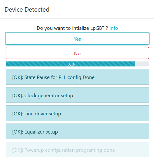
The spinner in the top right corner of the interface turns green when the LpGBT is locked.

You can start navigating the PiGBT web interface and configure the LpGBT. To scroll the PiGBT web interface menu click on the button in the left corner of the navigation bar. To reset the LpGBT click on the yellow reset button and to disable both VLDB+ FEASTMPs of the VLDB+ click on the green FEAST button.

3.2. LpGBT mode
3.2.1. Transceiver configuration
The LpGBT communicates with the counting room through optical links. You can configure LpGBT data transmission mode in the Chip Mode section. If you select the TX button, the LpGBT will work as a simple link transmitter for the uplink receiving the data to be transmitted from the front-end modules through the eLinks. If you select the RX button, the LpGBT will work as a simple link receiver, receiving data and clock reference from the counting room through the downlink. And if you select the TRX button, the LpGBT will work as a full link transceiver with bidirectional data communication with the front-ends and the counting room.
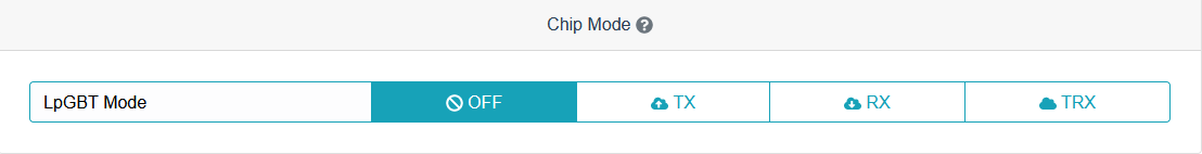
Note
Once the PiGBT Control ToolKit is connected to the VLDB+, you have to set the Mode[3:0] only through the PiGBT web interface. Physical changes on the SW7 will have no effect.
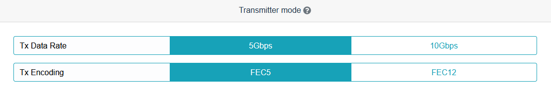
3.2.2. Transmitter configuration
The link from the counting room to the LpGBT is called downlink and its bandwidth is 2.56 Gb/s. The link from the LpGBT to the counting room is called uplink and its bandwidth can be set to 5.12 Gb/s or 10.24 Gb/s. Both links use Forward Error Correction (FEC) to detect and correct transmission errors. In the Transmitter mode section, you can select an uplink data rate of 5.12 Gb/s or 10.24 Gb/s together with a Forward Correction Error of FEC12 or FEC5, allowing to correct up to 12 or 5 bits respectively.
3.3. Elink groups
The EPTX window is subdivided into 7 groups and the EPRX window is subdivided into 4 groups. These groups contain 4 channels each. The data rate of each group can be set independently. The maximum and minimum data rates on each EPRX group will depend of the lpGBT’s high-speed mode of operation. You can configure the EPTX (downlink) and EPRX (uplink) eLinks on their corresponding window. Depending on the selected datarate for each group, the PiGBT will automatically set and unset the allowed channel(s) to drive it.
You can access the advanced configuration of each TX/RX Elink channel by clicking on the settings icon.

3.4. Clocks
3.4.1. Phase shifter clocks
The LpGBT ASIC provides 4 differential clock outputs that can be used as local timing references for the front-end modules. These clocks are generated by the phase-shifter circuit and can be controlled on the Clock section of the PiGBT menu. You can access to the advanced configuration of each PSClock channel by clicking on the settings icon.

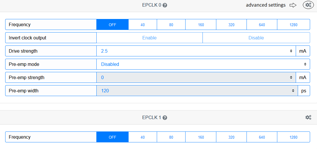
3.4.2. eLink clocks
The LpGBT chip features up to 29 independent clock outputs. Each ECLK output is independent and can be programmed with a frequency that goes from 0 to 1280 MHz. Each clock can be individually configured from PiGBT interface. You can access each ECLK advanced configuration by clicking on the settings icon.
3.5. High-speed links
On the High-Speed settings, the high-speed links polarity can be inverted in the uplink and downlink direction independently.

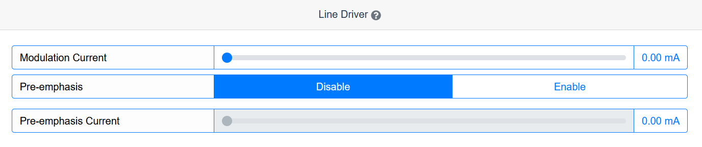
3.5.1. Line driver
On the line driver section of the High-speed settings, you can drive the transmission line that connects the LpGBT ASIC transmitter with the laser driver.
3.5.2. Equalizer
To help to optimize the equalizer response, the LpGBT has several features that can be involved in the process of selecting the best combination of capacitance and resistance. These parameters can be set on the Equalizer section of the High-speed settings.

3.5.3. Perform Eye-Diagram measurement
The Eye-Opening Monitor (EOM) block allows the user to make an on-chip Eye-Diagram measurement of the incoming 2.56 Gb/s high-speed data. Click on the Measure button to perform an Eye Opening Monitor. This action will take around 10 seconds to show a .jgp image that can be saved.
3.6. Test features
The LpGBT offers a variety of link test features: loopbacks, test pattern generators, pattern checkers all accessible on Test Features Menu.
You have the possibility to generate patterns and inject them at various places in the uplink and downlink data path. If any of the pattern generators is enabled, the user data from ePortRx or from the downlink frame are discarded. All generators are independent of each other and can be used at the same time.
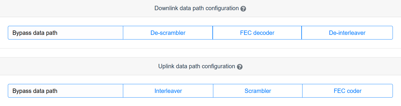
For testing purposes, de-interleaver, FEC decoder, and de-scrambler in the downlink data path can be bypassed. As well, interleaver, scrambler, and FEC coder in the uplink data path can be bypassed. Select an item to disable it.
3.6.1. Uplink data path test pattern
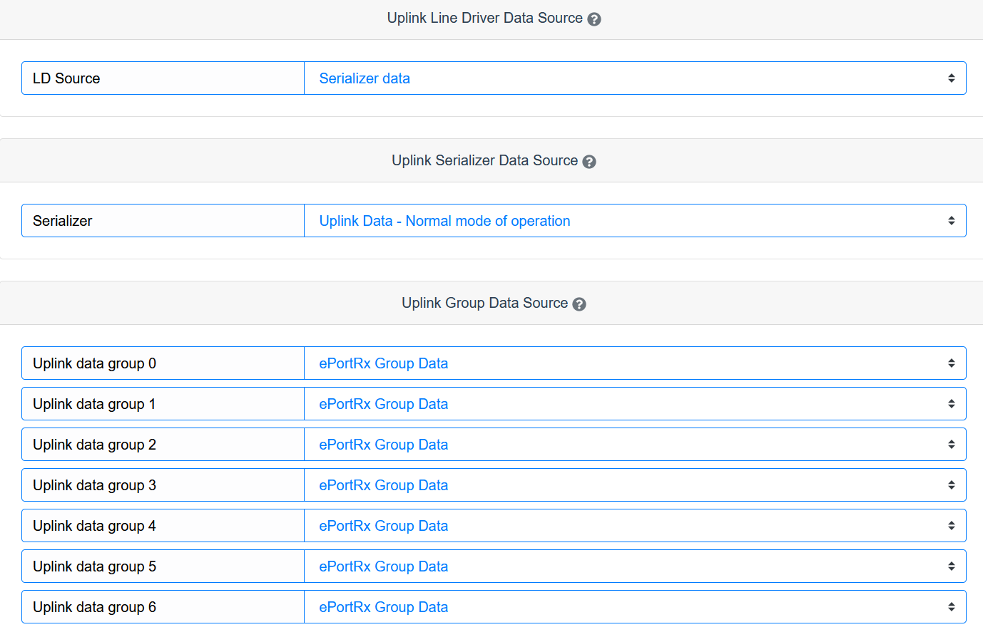
The LpGBT transmitter can be programmed on the Uplink Data Source section to transmit the following: a fixed pattern, PRBS sequence, clock sequence, or loopback incoming downlink frame. There is a PRBS generator included at each ePortRx input and can be configured on EPRX Group Channel PRBS Enable section.
3.6.2. Downlink data path test pattern
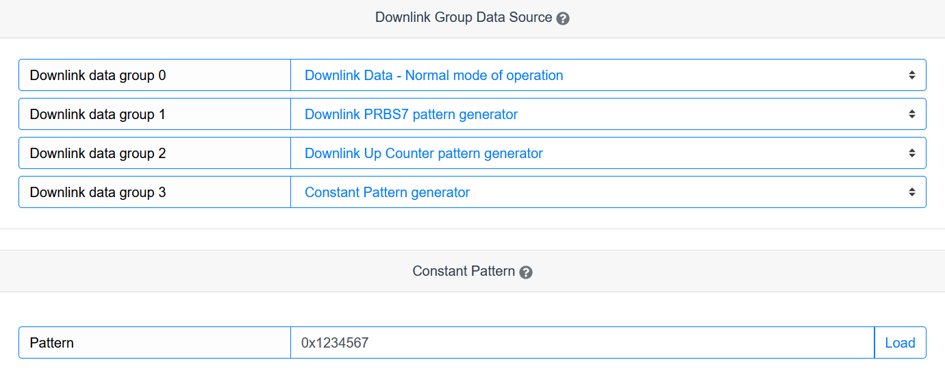
The data coming from the downlink frame to each ePortTx group can be tested and replaced with a test patterns. The test pattern for each group can be controlled independently.
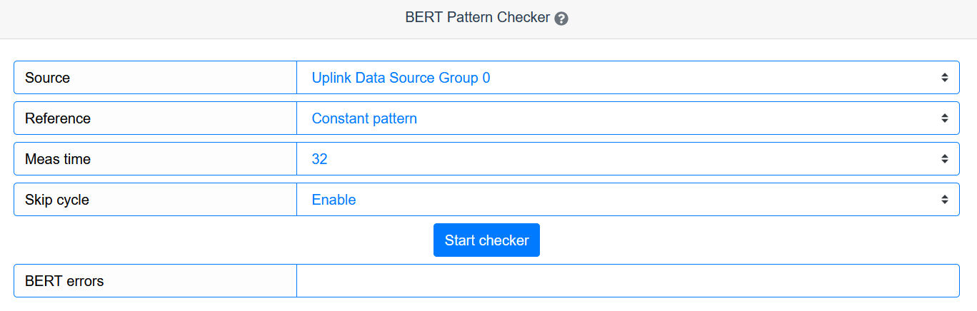
3.6.3. Bert checker
The LpGBT has one pattern checker which can monitor various points. The duration of the measurement is expressed in the number of 40 MHz clock cycles and can be programmed.
3.7. I2C Master
The three independent I2C masters (M0, M1, M2) are accessible from the I2C Master menu. You can configure which Master you want to use (Master number, slave address, register address width, address width, bus speed) and launch different types of I2C transactions: write and read data from any device connected to I2C master line.
Warning
Set I2C Master parameters in hexadecimal value (ex : 0xAA or AA)
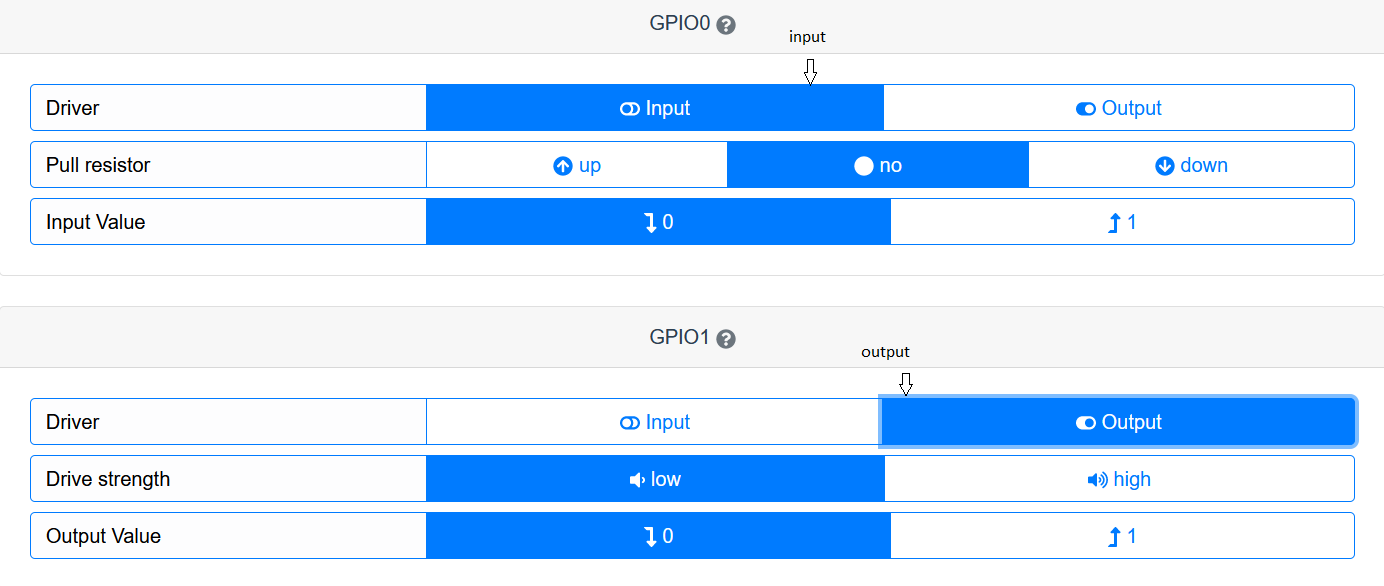
3.8. GPIO
The LpGBT has 16 I/O pins logically divided into two ports: Low and High. These pins can be driven from the GPIO section of the piGBT menu. Each port pin can be configured as input or output with configurable driver and pull settings.
3.9. Analog peripherals
The LpGBT has a built-in reference voltage generator which is shared between ADC and voltage DAC. Before playing with the ADC and DAC features, the internal voltage reference has to be enabled and be set to 1 V (typical value). The tune of the reference voltage can be performed by adjusting the VREF Tune slider.

3.9.1. Voltage Digital to Analog Converter
The LpGBT has a 12-bit R-2R voltage DAC. The DAC uses VREF voltage as a reference and thus can produce voltages ranging from 0 to VREF. Use the slider to tune voltage

3.9.2. Current Digital to Analog Converter
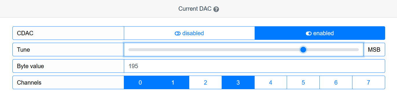
The 8 ADC inputs feature a switchable current source. This feature can be used to measure externally connected resistances. The current DAC can be enabled by setting the CDAC button. The current can be programmed from 0 to 0.8 mA using an 8 bit current DAC by setting the Tune slider. The current driver on each ADC channel can be set independently on the Channels area.
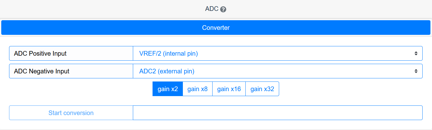
3.9.3. Analog to Digital Converter
In this section, you can configure the ADC block and perform a 10-bit analog to digital conversion. Select the input from the list of 16 multiplexed inputs available (out of which 8 are external), select the gain stage, and start conversion.
Note
The output of the sliders is set just once the slider is released.
3.10. Test outputs
The lpGBT chip has 6 test outputs, four of which are CMOS and two are differential. These can be configured in the Test Outputs window. Each signal can be connected to one of a number of different internal signals. These are selected in the drop-down named signal.

3.11. Registers
3.11.1. Save data to a file
To save the values of the LpGBT registers (317 writable registers) through the PiGBT web service, click on the Save button of the Registers window.

3.11.2. Fetch data from a file
To load the writable LpGBT registers through the PiGBT web service click on the Load button of Registers page and upload your .cnf file. The software will automatically update the LpGBT register values from it.

3.11.3. Fuse registers
You can fuse your LpGBT from the PiGBT interface. E-Fuse programming requires the pin VDDF2V5 to be powered at 2.5V. This power is only supplied during programming. The ribbon cable must be connected between the VLDB+ and RPI during the fusing process. Connect the left pin of the VLDB+ W16 jumper to the 2.5 V pin of the RPI Translator Board J2 using a cable.
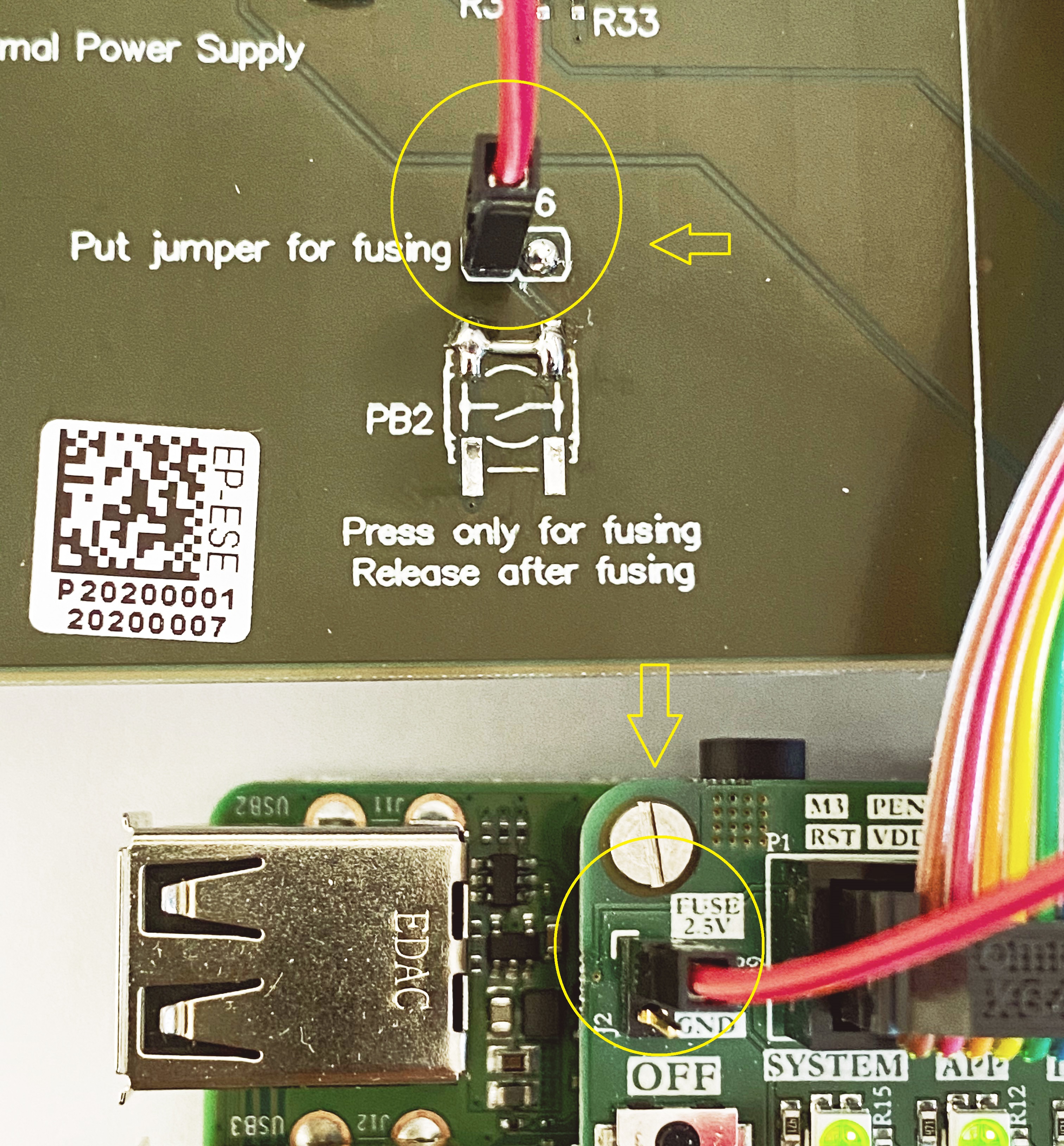
Note
The VLDB+ team has fused each VLDB+ USERID0 with each corresponding VLDB+ serial number to ensure that the fusing process from the PiGBT web application works.
The LpGBT must be in the Ready state to be fused. Before fusing your lpGBT, you have to configure it with your desired configuration to fuse. Then, you have to click on Fusing, located in the Registers window. Afterwards, you have to follow a process of three steps:
1 - It’s mandatory to have your LpGBT on Ready state for fusing. The PiGBT will ensure your LpGBT is on Ready state. In the case where your configuration doesn’t make your LpGBT to be on Ready state, please review it before fusing. In the case you don’t have a system (back-end, fibers…) to make it Ready, a warning window will appear. If you click OK, the PiGBT will force the lpGBT to be on Ready state.
2 - The PiGBT then reads the e-fuse banks. It will list all the already fused registers and if any register that you are going to fuse it’s already fused. Click on Continue if you are okay with that or the X button to cancel.
3 - Finally, after clicking on Continue, the 2.5 V will be automatically powered, the fusing sequence will start and the 2.5 V will also automatically stop.
You can ensure that you have fused your lpGBT by clicking on Fusing once more and stop on the 2nd step of the process where you read the fused registers


3.12. Connection
3.12.1. Cascaded lpGBT(s)
As mentioned in Section 3.1, the first thing to do to control the lpGBT is to select Real lpGBT target and select its address. After this, there is an additional possibility which implies a second lpGBT: in case the Real lpGBT has a second cascaded lpGBT through one of its I2CM, the PiGBT offers the possibility to directly control this cascaded lpGBT through the web interface. To do so, after having selected the address of the Real lpGBT, go to Connection and select Cascaded lpGBT. You will have to choose the I2CM of the Real lpGBT which your cascaded lpGBT is connected. Then, manually put the address of the cascaded lpGBT which you want to control. In case the status icon on the top right is red, then the cascaded lpGBT is not being detected by the Real lpGBT. In case the Real lpGBT detects the cascaded lpGBT, the status icon will be either yellow (cascaded lpGBT not in Ready state) or green (cascaded lpGBT in Ready state). In this target mode, the whole web interface will be linked to this cascaded lpGBT. You can navigate through the PiGBT in this target mode and control directly the cascaded lpGBT until you change to other Target mode in the Connection window.

Warning
Since in the Cascaded lpGBT target mode there are two I2C communications cascaded implied, the PiGBT web interface may be slower than expected.